
Wafers are the most basic semiconductor materials for making ICs. The quality of wafers will directly determine the quality of IC products. Due to different process levels, wafers may have defects in redundancy, crystal defects, and mechanical damage during the production process. Wafer inspection equipment is mainly used for the appearance inspection after wafer cutting, such as: size, breakage, cracking, pores, cracks, poor nickel layer and so on. Therefore, efficient and accurate inspection equipment is a guarantee for providing highly reliable wafer materials. Compared with traditional manual inspection, machine vision inspection has the advantages of high precision, high efficiency, continuity and non-contact pollution avoidance.
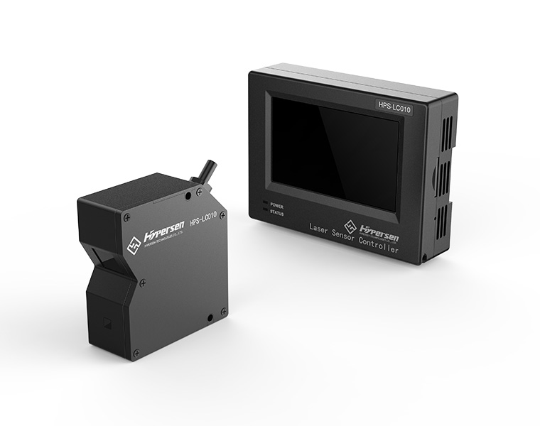
The high-precision HPS-LC010 laser displacement sensor developed by Hypersen can achieve ultra-high repeatability of ±0.1μm through non-contact detection, and is suitable for Z-axis high-precision positioning of pattern wafers.

Copyright 2020 All Rights Reserved.Hypersen Technologies Co., Ltd. haibosenc
